


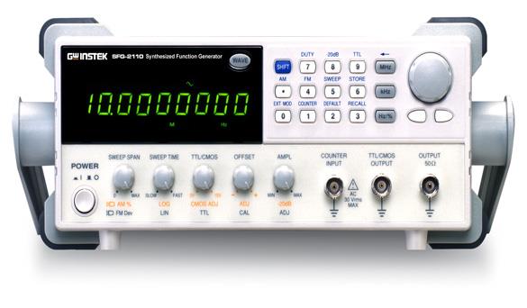
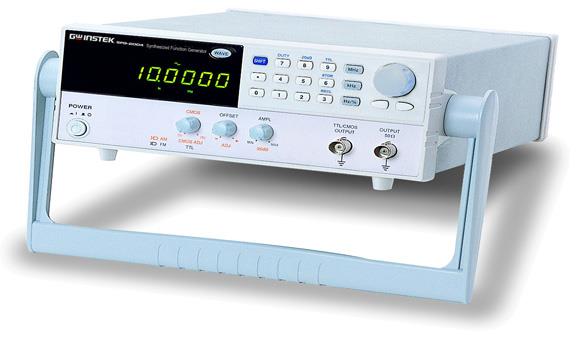
Direct digital Synthesis Technology and FPGA Chip Design
Frequency range :0.1Hz to 10MHz
Frequency resolution :100mHz
Frequency accuracy and drift: /-20ppm
Low distortion sine wave :-55 DBC,0.1Hz~200kHz
Output waveform: sine wave, square wave, triangle wave
TTL and CMOS OUT
The front panel can be configured with ten sets of storage and call operation memory
| Specifications | |
| Main output | |
| Frequency range (sine wave, square wave) | 0.1Hz~10MHz |
| Frequency range (triangular wave) | 0.1Hz~1MHz |
| The resolution | 0.1Hz |
| Frequency stability | ± 20 ppm |
| Frequency accuracy | ± 20 ppm |
| Long time accuracy | ± 5 ppm / year |
| Waveform type | Sine wave, square wave, triangle wave |
| Output amplitude | 10Vpp(including 50Ω load) |
| Amplitude to frequency flatness (relative to 1kHz sine wave) | <± 0.3dB,0.1Hz~1MHz; <± 0.5dB,1MHz~4MHz; <± 2dB, 4MHz~10MHz |
| Output impedance | 50Ω±10% |
| Output attenuator | -20dB±1dB×2 |
| Dc offset range | < -5V ~ > 5V(including 50Ω load) |
| Cycle ratio adjustment range | 20percent to 80percent below 1MHz (square wave only) |
| 周期比The resolution | 1% |
| Frequency disy | 9 digit LED disy |
| Sine wave | |
| Harmonic distortion | -55dBc,0.1Hz~200kHz; -40dBc,0.2MHz~4MHz; -30dBc,4MHz~10MHz(此为Output level值到十分之一值之Specifications且TTL/CMOS OFF) |
| Triangular wave | |
| Linearity | ≧98%,0.1Hz~100kHz;≧95%,100kHz~1MHz |
| Square wave | |
| Symmetry | ± 1percent of period 4ns to 0.1Hz ~ 100kHz; ± 1percent of period 4ns to 0.1Hz ~ 100khz; Rising and falling time: ≦25ns At maximum output (including 50Ω load) |
| CMOS output | |
| Output level | 4Vpp±1Vpp ~ 14.5Vpp±0.5Vpp adjustable; Rise and fall time: ≦120ns |
| TTL Output | |
| Output level | ≧3Vpp ; Output thrust: 20 TTL load; Rise and fall time: ≦25ns |
| Memory storage | |
| Store and call function | 10 sets of set memory |
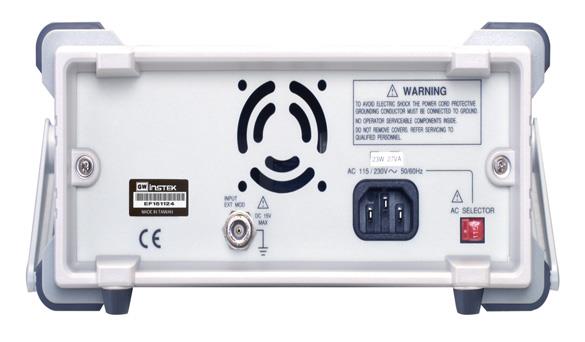
| Input power | |
|
|
AC115V, 230V±15%, 50/60Hz |
| Attachment | |
|
|
Operation manual ×1; Power cable x 1; GTL-101×1 |
| Appearance dimension | |
|
|
107(W)×266(H)×293(D) m/m;Approx. 3.1kg |

