


Product Overview
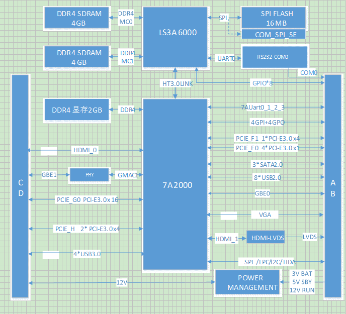
SMLS 3A7A H Module is designed according to PICMG COM Express Module Base Specification Reversion 2.0 Type 6,CPU The 3A6000 processor adopts four high-performance 6-emission 64-bit LA664 processor cores, and supports multi-thread technology (SMT2) to achieve four cores and eight threads, and is expected to be 2.5GHz (TDP, subject to the final specifications of the original factory). Equipped with Loongson's new generation of autonomous bridge chip 7A2000, integrated high-performance GPU disy function; 8GB of on-board DDR4 memory is standard. Module support 2 Gigabit network,32 PCI-E,8 USB2.0,4 USB3.0,6 serial ports,3 SATA3.0 and other I/O expansion; Supports three disy outputs: one HDMI/VGA port and one dual-channel 24-bit LVDS (HDMI optional) signal.
The module size is 95*95mm, typical power consumption is 35W (TDP), and the default is 100percent domestic. Module definition is fully compatible with JDA's previous generation SMLS 3A7A B/C/D/E series COM-E module, using full table attached design, with high performance, high localization, high stability, high reliability and other characteristics, can be widely used in national defense, government, scientific research, medical, electric power, communication, transportation and other fields
Product Features
Ø Using Loongson quad-core 3A6000 processor,7A2000 bridge;
Ø Standard onboard 8GB DDR4 memory particles;
Ø Support 1 HDMI interface and 1 VGA, copy screen mode; 1 dual channel LVDS interface (optional HDMI), resolution support 1920*1080;
Ø Support onboard 2 Gigabit network interface,3 SATA3.0;
Support 2 channels PCI-E3.0x8,3 channels PCI-E3.0x4,4 channels PCI-E2.0x1;
Ø Support 8 USB2.0,4 USB3.0;
Ø Support 1 RS232 debugging serial port,1 SE RS232 debugging serial port,4 TTL serial port;
Ø Support 1 HDA audio interface;
Ø Support SPI,LPC,2 I2C and other interfaces;
Ø Localization rate of components 100percent.
Product specifications
Project |
Description |
|
Processor |
CPU |
龙芯四核3A6000Processor |
Main frequency |
默认Main frequency2.5GHz(以原厂测试为准) |
|
Chipset |
Bridge te |
Loongson 7A2000, integrated autonomous GPU, DDR4 2GB |
Memory |
Type |
Onboard DDR4 |
Capacity |
8GB |
|
Trusted root |
Credible SE |
Reserve support |
Debugging |
Debugging串口pin座 |
1路板载CPU RS232Debugging串口; 1路板载SE RS232Debugging串口; |
Expansion interface |
PCIE |
Supports 32 PCIE lanes. Software configuration is supported. The default allocation is as follows G0: Two PCI-E3.0x8 channels are standard H: Two PCI-Ex4 channels are configured as standard, and one PCI-Ex8 channels are optional F1: Standard with one PCI-E3.0x4, optional with two PCI-Ex1 F0: Four PCI-E2.0x1 channels are configured as standard, and one PCI-Ex4-- is optional |
USB |
Eight USB2.0 ports, four USB3.0 ports |
|
SATA |
Three SATA3.0 ports |
|
Ethernet |
Two 10/100/1000Mb adaptive Gigabit network ports (GBe1 is temporarily unavailable) |
|
Audio |
Route 1 HDA |
|
Disy |
1 HDMI,1 VGA, copy screen mode 1 channel 24bit LVDS, resolution 1920*1080 |
|
LPC |
1 LPC channel |
|
SPI |
1 SPI channel, support 3 slice selection (peripheral) |
|
I²C |
Two I²C channels |
|
Serial |
4-channel 7A uart0/1/2/3 TTL serial port |
|
GPIO |
4 GPI,4 GPO |
|
Power supply |
Type |
3.0V RTC,5V Standby and 12V Primary |
Power consumption |
模块典型Power consumption(TDP 35w) |
|
Physical parameters |
Size (W×D) |
95x95mm |
Environmental adaptability |
Room temperature grade |
Operating temperature: 0℃-40℃,5-95percent RH, non-condensing |
Storage temperature: -20℃-70℃,5-95percent RH, non-condensing |
||
Wide temperature level |
Operating temperature: -20℃-60℃,5-95percent RH, non-condensing |
|
Storage temperature: -40℃-75℃,5-95percent RH, non-condensing |
||
Industrial grade |
Operating temperature: -40℃-65℃,5-95percent RH, non-condensing |
|
Storage temperature: -55℃-80℃,5-95percent RH, non-condensing |
||
Product function block diagram
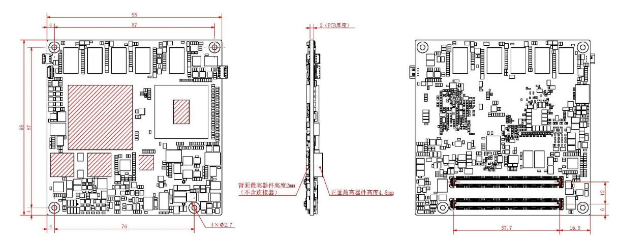
Product structure
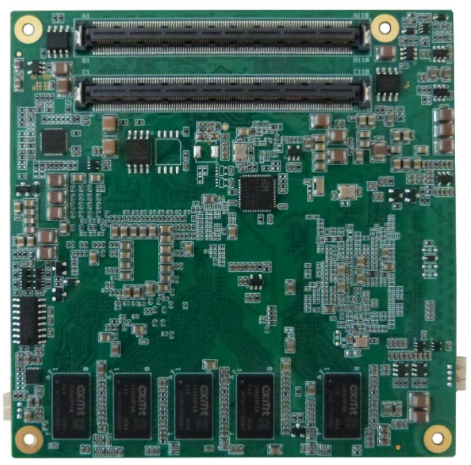
Appearance view


Outline size drawing
Heat dissipation requirements
The module requires a heat sink to dissipate heat. It can dissipate heat passively or actively. Figure 2-4 shows the position of the thermal conductive device:
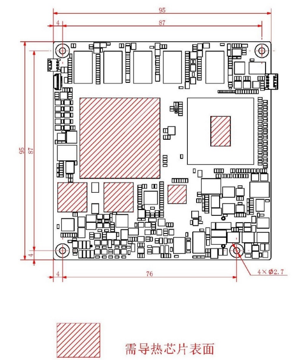
Cooling device identification diagram
Motherboard screen printing rules
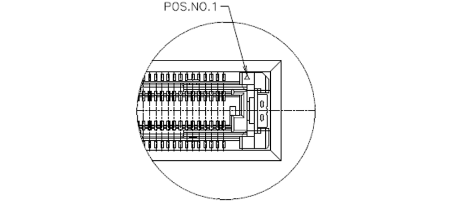
How to identify jumper, interface first pin?
a. Observe the plug, the text mark next to the socket: usually use "1" or bold line or triangle symbol "△" to indicate
b. Look at the pad on the back, usually the square pad is the first foot
c. The A1/C1 pins of the 220Pin te-to-board connector are located at the diagonal opening of the connector as shown in the following figure. Pin B1/D1 is on the opposite side of pin A1/C1
Module connector Definition
Pin identification diagram
Interface Definition Description
The interface of this module adopts two groups of 220pin high-reliability board-to-board COM-E connectors.
Module end model: NGTA21-1220-0601-01C/158CQSL-110-01-L-D-A/TE3-6318490-6;
Base te end model: NGTA21-2220-0601-01C/158CQTL-110-01-L-D-A (5mm) /TE1827253 C1 (5mm) /TE3-6318491-6 (8mm)
The PIN of the COMe interface [MD1-MD2] is defined in the following table:
Table 3 1 Module COMe interface definition table
Serial number |
MD1 [NGT A21-1220-0601-01C] |
MD2 [NGT A21-1220-0601-01C] |
||
Row A |
Row B |
Row C |
Row D |
|
1 |
GND(FIXED) |
GND(FIXED) |
GND(FIXED) |
GND(FIXED) |
2 |
GBE0_MDI3-(Suspend) |
GBE0_ACT#(Suspend) |
GND |
GND |
3 |
GBE0_MDI3+(Suspend) |
LPC_FRAME# |
GBE1_MDI3-(Suspend) |
GBE1_LINK100#(Suspend) |
4 |
GBE0_LINK100#(Suspend) |
LPC_AD0 |
GBE1_MDI3+(Suspend) |
GBE1_ACT#(Suspend) |
5 |
GBE0_LINK1000#(Suspend) |
LPC_AD1 |
GND |
GND |
6 |
GBE0_MDI2-(Suspend) |
LPC_AD2 |
GBE1_MDI2-(Suspend) |
GBE1_LINK1000#(Suspend) |
7 |
GBE0_MDI2+(Suspend) |
LPC_AD3 |
GBE1_MDI2+(Suspend) |
GBE1_LINK#(Suspend) |
8 |
GBE0_LINK#(Suspend) |
7A_ACPI_GPIO12(Suspend) |
GND |
GND |
9 |
GBE0_MDI1-(Suspend) |
7A_ACPI_GPIO13(Suspend) |
GBE1_MDI1-(Suspend) |
PCIE_H_RX6_P |
10 |
GBE0_MDI1+(Suspend) |
LPC_CLK |
GBE1_MDI1+(Suspend) |
PCIE_H_RX6_N |
11 |
GND(FIXED) |
GND(FIXED) |
GND(FIXED) |
GND(FIXED) |
12 |
GBE0_MDI0-(Suspend) |
PWRBTN#(Suspend) |
GBE1_MDI0-(Suspend) |
PCIE_H_RX7_P |
13 |
GBE0_MDI0+(Suspend) |
LS7A_I2C1_SCL |
GBE1_MDI0+(Suspend) |
PCIE_H_RX7_N |
14 |
VCC_1V8(Fix) |
LS7A_I2C1_SDA |
GND |
GND |
15 |
SUS_S3#(Suspend) |
SMB_ALERT# |
PCIE_H_RX2+ |
PCIE_H _TX0+ |
16 |
SATA0_TX+ |
SATA1_TX+ |
PCIE_H _RX2- |
PCIE_H _TX0- |
17 |
SATA0_TX- |
SATA1_TX- |
SUSB0_RX- |
SUSB0_TX- |
18 |
SUS_S4#(Suspend) |
SUS_STAT#(Suspend) |
SUSB0_RX+ |
SUSB0_TX+ |
19 |
SATA0_RX+ |
SATA1_RX+ |
PEF1_RX2+ |
PEF1_TX2+ |
20 |
SATA0_RX- |
SATA1_RX- |
PEF1_RX2- |
PEF1_TX2- |
21 |
GND(FIXED) |
GND(FIXED) |
GND(FIXED) |
GND(FIXED) |
22 |
SATA2_TX+ |
PCIE_H_RX4_P |
PEF1_RX3+ |
PEF1_TX3+ |
23 |
SATA2_TX- |
PCIE_H_RX4_N |
PEF1_RX3- |
PEF1_TX3- |
24 |
SUS_S5#(Suspend) |
PWR_OK |
LS7A_UART2_TXD |
SUSB1_TX- |
25 |
SATA2_RX+ |
PCIE_H_RX5_P |
PCIE_H _RX3+ |
SUSB1_TX+ |
26 |
SATA2_RX- |
PCIE_H_RX5_N |
PCIE_H _RX3- |
PCIE_H _TX1+ |
27 |
BATLOW#(Suspend) |
WDT |
SUSB1_RX- |
PCIE_H _TX1- |
28 |
(S)ATA_ACT# |
HDA_SDIN2 |
SUSB1_RX+ |
NC |
29 |
HDA_SYNC |
HDA_SDIN1 |
PCIE_H _RX1+ |
PCIE_H _TX2+ |
30 |
HDA_RST# |
HDA_SDIN0 |
PCIE_H _RX1- |
PCIE_H _TX2- |
31 |
GND(FIXED) |
GND(FIXED) |
GND(FIXED) |
GND(FIXED) |
32 |
HDA_BITCLK |
SPKR |
SUSB2_RX- |
PCIE_H _TX3+ |
33 |
HDA_SDOUT |
LS7A_I2C0_SCL |
SUSB2_RX+ |
PCIE_H _TX3- |
34 |
NC |
LS7A_I2C0_SDA |
SUSB3_RX- |
SUSB2_TX- |
35 |
THRMTRIP# |
THRM# |
SUSB3_RX+ |
SUSB2_TX+ |
36 |
USB6-(Suspend) |
USB7-(Suspend) |
HDMI_CTRLCLK |
PCIE_H _RX0+ |
37 |
USB6+(Suspend) |
USB7+(Suspend) |
HDMI_CTRLDATA |
PCIE_H _RX0- |
38 |
USB_OC3#(Suspend) |
USB_OC2#(Suspend) |
LS7A_UART2_RXD |
NC |
39 |
USB4-(Suspend) |
USB5-( Suspend) |
HDMI_DATA2_P |
PCIE_H _TX4+ |
40 |
USB4+(Suspend) |
USB5+( Suspend) |
HDMI_DATA2_N |
PCIE_H _TX4- |
41 |
GND(FIXED) |
GND(FIXED) |
GND(FIXED) |
GND(FIXED) |
42 |
USB2-(Suspend) |
USB3-( Suspend) |
HDMI_DATA1_P |
PCIE_H _TX5+ |
43 |
USB2+(Suspend) |
USB3+( Suspend) |
HDMI_DATA1_N |
PCIE_H _TX5- |
44 |
USB_OC1# (Suspend) |
USB_OC0# (Suspend) |
HDMI_HPD |
SUSB3_TX- |
45 |
USB0-(Suspend) |
USB1-(Suspend) |
LS7A_UART3_TXD |
SUSB3_TX+ |
46 |
USB0+(Suspend) |
USB1+(Suspend) |
HDMI_DATA0_P |
PCIE_H _TX6+ |
47 |
VCC_RTC |
USB9-(Suspend) |
HDMI_DATA0_N |
PCIE_H _TX6- |
48 |
USB8-(Suspend) |
USB9+(Suspend) |
LS7A_UART3_RXD |
NC |
49 |
USB8+(Suspend) |
SYS_RESET#(Suspend) |
HDMI_CLK_P |
PCIE_H _TX7+ |
50 |
LPC_SERIRQ |
CB_RESET#(Suspend) |
HDMI_CLK_N |
PCIE_H _TX7- |
51 |
GND(FIXED) |
GND(FIXED) |
GND(FIXED) |
GND(FIXED) |
52 |
PEF1_TX1+ |
PEF1_RX1+ |
PEG0_RX0+ |
PEG0_TX0+ |
53 |
PEF1_TX1- |
PEF1_RX1- |
PEG0_RX0- |
PEG0_TX0- |
54 |
GPI0 |
GPO1 |
NC |
NC |
55 |
PEF1_TX0+ |
PEF1_RX0+ |
PEG0_RX1+ |
PEG0_TX1+ |
56 |
PEF1_TX0- |
PEF1_RX0- |
PEG0_RX1- |
PEG0_TX1- |
57 |
GND |
GPO2 |
NC |
NC |
58 |
PEF0_TX3+ |
PEF0_RX3+ |
PEG0_RX2+ |
PEG0_TX2+ |
59 |
PEF0_TX3- |
PEF0_RX3- |
PEG0_RX2- |
PEG0_TX2- |
60 |
GND(FIXED) |
GND(FIXED) |
GND(FIXED) |
GND(FIXED) |
61 |
PEF0_TX2+ |
PEF0_RX2+ |
PEG0_RX3+ |
PEG0_TX3+ |
62 |
PEF0_TX2- |
PEF0_RX2- |
PEG0_RX3- |
PEG0_TX3- |
63 |
GPI1 |
GPO3 |
LS3A_COM0_TX(RS232) |
USB11-(Suspend) |
64 |
PEF0_TX1+ |
PEF0_RX1+ |
LS3A_COM0_RX(RS232) |
USB11+(Suspend) |
65 |
PEF0_TX1- |
PEF0_RX1- |
PEG0_RX4+ |
PEG0_TX4+ |
66 |
GND |
WAKE0#(Suspend) |
PEG0_RX4- |
PEG0_TX4- |
67 |
GPI2 |
WAKE1#(Suspend) |
NC |
GND |
68 |
PEF0_TX0+ |
PEF0_RX0+ |
PEG0_RX5+ |
PEG0_TX5+ |
69 |
PEF0_TX0- |
PEF0_RX0- |
PEG0_RX5- |
PEG0_TX5- |
70 |
GND(FIXED) |
GND(FIXED) |
GND(FIXED) |
GND(FIXED) |
71 |
LVDS_A0+ |
LVDS_B0+ |
PEG0_RX6+ |
PEG0_TX6+ |
72 |
LVDS_A0- |
LVDS_B0- |
PEG0_RX6- |
PEG0_TX6- |
73 |
LVDS_A1+ |
LVDS_B1+ |
GND |
GND |
74 |
LVDS_A1- |
LVDS_B1- |
PEG0_RX7+ |
PEG0_TX7+ |
75 |
LVDS_A2+ |
LVDS_B2+ |
PEG0_RX7- |
PEG0_TX7- |
76 |
LVDS_A2- |
LVDS_B2- |
GND |
GND |
77 |
LVDS_VDD_EN |
LVDS_B3+ |
NC |
NC |
78 |
LVDS_A3+ |
LVDS_B3- |
PEG0_RX8+ |
PEG0_TX8+ |
79 |
LVDS_A3- |
LVDS_BKLT_EN |
PEG0_RX8- |
PEG0_TX8- |
80 |
GND(FIXED) |
GND(FIXED) |
GND(FIXED) |
GND(FIXED) |
81 |
LVDS_A_CK+ |
LVDS_B_CK+ |
PEG0_RX9+ |
PEG0_TX9+ |
82 |
LVDS_A_CK- |
LVDS_B_CK- |
PEG0_RX9- |
PEG0_TX9- |
83 |
LVDS_I2C_CK |
LVDS_BKLT_CTRL |
NC |
NC |
84 |
LVDS_I2C_DAT |
VCC_5V_SBY |
GND |
GND |
85 |
GPI3 |
VCC_5V_SBY |
PEG0_RX10+ |
PEG0_TX10+ |
86 |
USB10-(Suspend) |
VCC_5V_SBY |
PEG0_RX10- |
PEG0_TX10- |
87 |
USB10+(Suspend) |
VCC_5V_SBY |
GND |
GND |
88 |
PCIE_CLK_REF+ |
7A_ACPI_GPIO04(Suspend) |
PEG0_RX11+ |
PEG0_TX11+ |
89 |
PCIE_CLK_REF- |
VGA_RED |
PEG0_RX11- |
PEG0_TX11- |
90 |
GND(FIXED) |
GND (FIXED) |
GND(FIXED) |
GND(FIXED) |
91 |
SPI_POWER |
VGA_GRN |
PEG0_RX12+ |
PEG0_TX12+ |
92 |
SPI_MISO |
VGA_BLU |
PEG0_RX12- |
PEG0_TX12- |
93 |
GPO0 |
VGA_HSYNC |
GND |
GND |
94 |
SPI_CLK |
VGA_VSYNC |
PEG0_RX13+ |
PEG0_TX13+ |
95 |
SPI_MOSI |
VGA_I2C_CK |
PEG0_RX13- |
PEG0_TX13- |
96 |
TPM_PP |
VGA_I2C_DAT |
GND |
GND |
97 |
NC |
LS7A_SPI_CS1# |
SPI_CS2# |
SPI_CS3# |
98 |
LS7A_UART0_TXD |
NC |
PEG0_RX14+ |
PEG0_TX14+ |
99 |
LS7A_UART0_RXD |
7A1000_SCI# |
PEG0_RX14- |
PEG0_TX14- |
100 |
GND(FIXED) |
GND(FIXED) |
GND(FIXED) |
GND(FIXED) |
101 |
LS7A_UART1_TXD |
FAN_PWMOUT |
PEG0_RX15+ |
PEG0_TX15+ |
102 |
LS7A_UART1_RXD |
FAN_TACHIN |
PEG0_RX15- |
PEG0_TX15- |
103 |
LS7A_ACPI_LID#(Suspend) |
7A_ACPI_GPIO02(Suspend) |
GND |
GND |
104 |
VCC_12V |
VCC_12V |
VCC_12V |
VCC_12V |
105 |
VCC_12V |
VCC_12V |
VCC_12V |
VCC_12V |
106 |
VCC_12V |
VCC_12V |
VCC_12V |
VCC_12V |
107 |
VCC_12V |
VCC_12V |
VCC_12V |
VCC_12V |
108 |
VCC_12V |
VCC_12V |
VCC_12V |
VCC_12V |
109 |
VCC_12V |
VCC_12V |
VCC_12V |
VCC_12V |
110 |
GND(FIXED) |
GND(FIXED) |
GND(FIXED) |
GND(FIXED) |
Other interface connectors
Serial port 1 Connector Definition [CN2]
Table 3 2 Definition of serial port connectors
Serial number |
Definition |
Note |
1 |
RXD1 |
LS3A6000_RS232Debugging串口 |
2 |
TXD1 |
|
3 |
GND |
|

