


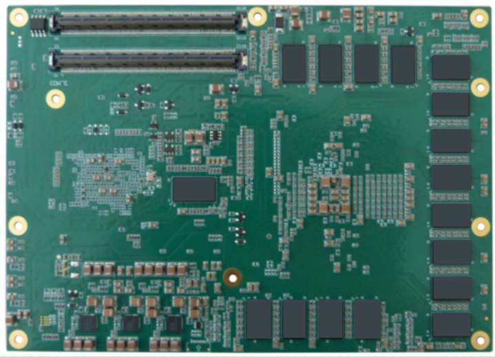
Product Overview
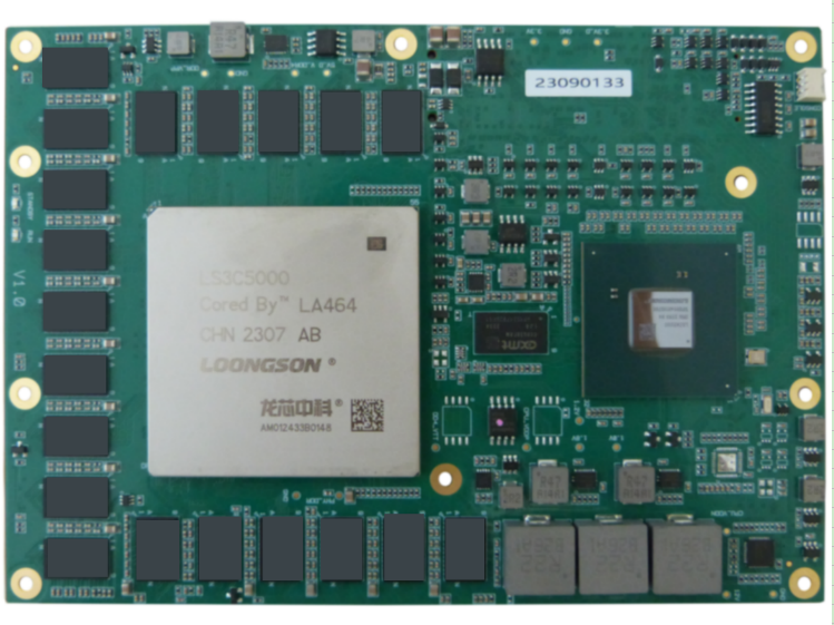
The SMLS 3C7A Module is designed according to PICMG COM Express Module Base Specification Reversion 2.0Type 7 Extended Modules. The CPU adopts Loongson high-performance server 16-core processor LS3C5000, the default frequency is 2.0GHz; Equipped with Loongson's new generation of autonomous bridge chip 7A2000, integrated high-performance GPU disy function; The standard on-board 32GB DDR4 memory supports the ECC function. Module support 2 Gigabit network,4 USB2.0,4 USB3.0,6 serial ports,4 SATA3.0 and other I/O expansion; PCIE standard configuration supports two PCIE3.0x8, three pcie 3.0x4, four pcie 2.0X1, and four pcie clock outputs. The disy port supports 1 HDMI0 VGA disy and 1 HDMI.
The module size is COM-E Extended Modules standard size 110*155mm, typical power consumption 95W (TDP), the default 100percent of domestic. The components adopt full table attached design, with high performance, high localization, high stability, high reliability and other characteristics, can be widely used in national defense, government, scientific research, medical, electric power, communication, transportation and other fields
Product Features
² Using Loongson server 16-core processor 3C5000, frequency 2.0~2.2GHz,7A2000 bridge chip;
² Standard on-board 32GB DDR4 memory particles, support ECC;
² Default support for 4 SATA3.0 channels;
² Support 1 HDMI interface and 1 VGA, copy screen mode; 1 channel HDMI, resolution support 1920*1080;
² Support 2 Gigabit network interfaces on board;
² Support 2 channels PCI-E3.0x8,3 channels PCI-E3.0x4,4 channels PCI-E3.0x1,COME output with 4 groups of PCIE Clock;
² Support 4 USB2.0,4 USB3.0;
² Support 1 RS232 debugging serial port,4 TTL serial port;
² Support 1 HDA audio interface;
² Support SPI,LPC, 2-way I2C interface;
² Localization rate of components 100percent.
Product specifications
Project |
Description |
|
Processor |
CPU |
龙芯十六核3C5000Processor |
Main frequency |
默认Main frequency2.0GHz |
|
Chipset |
Bridge te |
Loongson 7A2000, integrated autonomous GPU, DDR4 2GB |
Memory |
Type |
On-board DDR432GB, support ECC |
Trusted root |
Credible SE |
Reserve support |
Expansion interface |
PCIE |
Supports 32 PCIE3.0 channels. Software configuration is supported. The default allocation is as follows G0: two channels of PCI-Ex8-- are standard H: Two PCI-Ex4 channels are configured as standard, and one PCI-Ex8 channels are optional F1: Standard with 1 PCI-Ex4 F0: four PCI-Ex1 channels are configured as standard, and one PCI-Ex4-- is optional Supports four PCIE clock outputs |
USB |
Four USB2.0 ports, four USB3.0 |
|
SATA |
Four SATA3.0 ports |
|
Ethernet |
Two 10/100/1000Mb Gigabit network ports (One GBE0 is used by default, and one GBE1 is reserved) |
|
Audio |
Route 1 HDA |
|
Disy |
1 HDMI 0,1 VGA, copy screen mode. Resolution 1920*1080 1 channel HDMI 1, resolution 1920*1080 |
|
LPC |
1 LPC channel |
|
SPI |
One SPI channel supports QSPI |
|
I²C |
Two I²C channels |
|
Serial |
Four TTL serial ports 1 on-board RS232 debugging serial port |
|
GPIO |
4 GPI,4 GPO |
|
Power supply |
Type |
3.0V RTC,5V Standby and 12V Primary |
Power consumption |
模块典型Power consumption(2.0GHz,TDP<95w) |
|
Physical parameters |
Size (W×D) |
110x155mm |
Environmental adaptability |
Room temperature grade |
Operating temperature: 10℃-40℃,5-95percent RH, non-condensing |
Storage temperature: -40℃-70℃,5-95percent RH, non-condensing |
||
Wide temperature level |
Operating temperature: -20℃-50℃,5-95percent RH, non-condensing |
|
Storage temperature: -40℃-70℃,5-95percent RH, non-condensing |
||
Industrial grade |
Operating temperature: -40℃-55℃,5-95percent RH, non-condensing |
|
Storage temperature: -40℃-70℃,5-95percent RH, non-condensing |
||

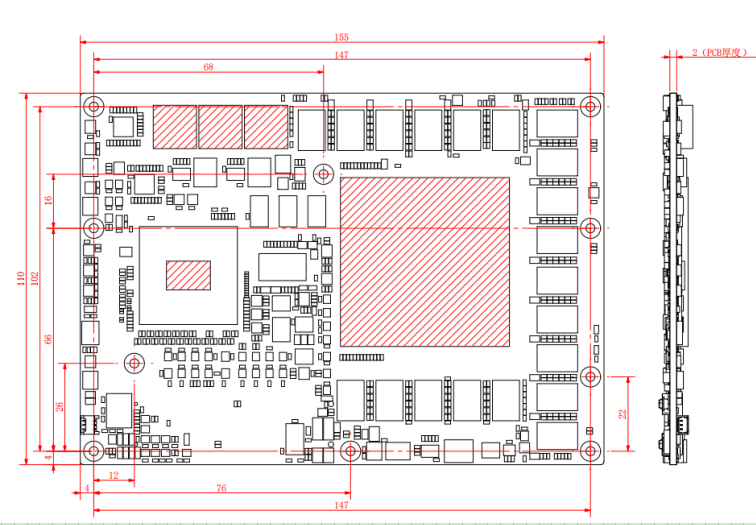
Appearance view

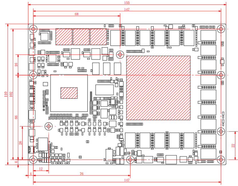
Structure size
Standard Extended Module size: 110 x 155mm

Heat dissipation design
模块Power consumption较高,需要散热器进行主动散热,接触导热器件位置如下图2-4示:
Motherboard screen printing rules
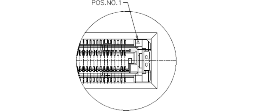
How to identify jumper, interface first pin?
a. Observe the plug, the text mark next to the socket: usually use "1" or bold line or triangle symbol "△";
b. Look at the pad on the back, usually the square pad is the first foot;
c. The A1/C1 pins of the 220Pin te-to-board connector are located at the diagonal opening of the connector as shown in the following figure. Feet B1/D1 are located opposite feet A1/C1.
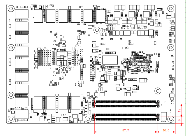
Interface Definition Description
The interface of this module adopts two groups of 220pin high-reliability board-to-board COM-E connectors.
Module end connector model: A21-1220-0601-01C; Base te end connector Model: A21-2220-0601-01C.
Table 3-1COM-E interface definitions
SMLS_3C7A_APin Assignment |
||||
Num |
Row A |
Row B |
Row C |
Row D |
1 |
GND |
GND (FIXED) |
GND (FIXED) |
GND (FIXED) |
2 |
GBE0_P3_N |
GBE0_ACT# |
GND |
GND |
3 |
GBE0_P3_P |
LPC_FRAME# |
SUSB0_RX_N |
SUSB0_TX_N |
4 |
GBE0_100M# |
LPC_AD0 |
SUSB0_RX_P |
SUSB0_TX_P |
5 |
GBE0_1000M# |
LPC_AD1 |
GND |
GND |
6 |
GBE0_P2_N |
LPC_AD2 |
SUSB1_RX_N |
SUSB1_TX_N |
7 |
GBE0_P2_P |
LPC_AD3 |
SUSB1_RX_P |
SUSB1_TX_P |
8 |
GBE0_LINK# |
RSVD_LVDS_BL_EN |
GND |
GND |
9 |
GBE0_P1_N |
RSVD_LVDS_VDD_EN |
SUSB2_RX_N |
SUSB2_TX_N |
10 |
GBE0_P1_P |
LPC_33M |
SUSB2_RX_P |
SUSB2_TX_P |
11 |
GND |
GND (FIXED) |
GND (FIXED) |
GND (FIXED) |
12 |
GBE0_P0_N |
PWRBTN# |
SUSB3_RX_N |
SUSB3_TX_N |
13 |
GBE0_P0_P |
I2C1_SCL |
SUSB3_RX_P |
SUSB3_TX_P |
14 |
VCC_CTREF(1.8V) |
I2C1_SDA |
GND |
GND |
15 |
SUS_S3# |
SMB_ALERT# |
PCIE_CK_REF1_P |
PCIE_CK_REF2_P |
16 |
SATA0_TX_P |
SATA1_TX_P |
PCIE_CK_REF1_N |
PCIE_CK_REF2_N |
17 |
SATA0_TX_N |
SATA1_TX_N |
GBE1_1000M# |
GBE1_100M# |
18 |
SUS_S4# |
SUSSTAT# |
GND |
GND |
19 |
SATA0_RX_P |
SATA1_RX_P |
PCIE_F1_RX2_P |
PCIE_F1_TX2_P |
20 |
SATA0_RX_N |
SATA1_RX_N |
PCIE_F1_RX2_N |
PCIE_F1_TX2_N |
21 |
GND |
GND (FIXED) |
GND (FIXED) |
GND (FIXED) |
22 |
PCIE_H_TX7_P |
PCIE_H_RX7_P |
PCIE_F1_RX3_P |
PCIE_F1_TX3_P |
23 |
PCIE_H_TX7_N |
PCIE_H_RX7_N |
PCIE_F1_RX3_N |
PCIE_F1_TX3_N |
24 |
SUS_S5# |
PSU_OK |
GBE1_LINK# |
GBE1_ACT# |
25 |
PCIE_H_TX6_P |
PCIE_H_RX6_P |
GND |
GND |
26 |
PCIE_H_TX6_N |
PCIE_H_RX6_N |
SATA2_TX_P |
SATA3_TX_P |
27 |
RSVD_TEST |
WDT |
SATA2_TX_N |
SATA3_TX_N |
28 |
SATA_ACT# |
HDA_SDI2 |
GND |
GND |
29 |
HDA_SYNC |
HDA_SDI1 |
SATA2_RX_P |
SATA3_RX_P |
30 |
HDA_RESET# |
HDA_SDI0 |
SATA2_RX_N |
SATA3_RX_N |
31 |
GND |
GND (FIXED) |
GND (FIXED) |
GND (FIXED) |
32 |
HDA_BITCLK |
SPKR |
GBE1_P0_N |
GBE1_P1_N |
33 |
HDA_SDO |
I2C0_SCL |
GBE1_P0_P |
GBE1_P1_P |
34 |
RSVD_TEST |
I2C0_SDA |
GBE1_P2_N |
GBE1_P3_N |
35 |
THERMTRIP# |
THRM# |
GBE1_P2_P |
GBE1_P3_P |
36 |
PCIE_H_TX5_P |
PCIE_H_RX5_P |
HDMI0_SCL |
HDMI1_SCL |
37 |
PCIE_H_TX5_N |
PCIE_H_RX5_N |
HDMI0_SDA |
HDMI1_SDA |
38 |
GND |
GND |
GND |
GND |
39 |
PCIE_H_TX4_P |
PCIE_H_RX4_P |
HDMI0_CLK_P |
HDMI1_CLK_P |
40 |
PCIE_H_TX4_N |
PCIE_H_RX4_N |
HDMI0_CLK_N |
HDMI1_CLK_N |
41 |
GND (FIXED) |
GND (FIXED) |
GND (FIXED) |
GND (FIXED) |
42 |
USB2_N |
USB3_N |
HDMI0_DATA0_P |
HDMI1_DATA0_P |
43 |
USB2_P |
USB3_P |
HDMI0_DATA0_N |
HDMI1_DATA0_N |
44 |
USB_OC1# |
USB_OC0# |
GND |
GND |
45 |
USB0_N |
USB1_N |
HDMI0_HPD |
HDMI1_HPD |
46 |
USB0_P |
USB1_P |
HDMI0_DATA1_P |
HDMI1_DATA1_P |
47 |
VCC_BAT |
USB5_N |
HDMI0_DATA1_N |
HDMI1_DATA1_N |
48 |
USB4_N |
USB5_P |
GND |
GND |
49 |
USB4_P |
SYS_RESETN# |
HDMI0_DATA2_P |
HDMI1_DATA2_P |
50 |
LPC_SERIRQ# |
CB_RESET# |
HDMI0_DATA2_N |
HDMI1_DATA2_N |
51 |
GND (FIXED) |
GND (FIXED) |
GND (FIXED) |
GND (FIXED) |
52 |
PCIE_F1_TX1_P |
PCIE_F1_RX1_P |
PCIE_G0_RX0_P |
PCIE_G0_TX0_P |
53 |
PCIE_F1_TX1_N |
PCIE_F1_RX1_N |
PCIE_G0_RX0_N |
PCIE_G0_TX0_N |
54 |
GPI0 |
GPO1 |
RSVD_SE_GPIO5 |
RSVD_SE_RS232_RX |
55 |
PCIE_F1_TX0_P |
PCIE_F1_RX0_P |
PCIE_G0_RX1_P |
PCIE_G0_TX1_P |
56 |
PCIE_F1_TX0_N |
PCIE_F1_RX0_N |
PCIE_G0_RX1_N |
PCIE_G0_TX1_N |
57 |
GND |
GPO2 |
RSVD_SE_GPIO6 |
RSVD_SE_RS232_TX |
58 |
PCIE_F0_TX3_P |
PCIE_F0_RX3_P |
PCIE_G0_RX2_P |
PCIE_G0_TX2_P |
59 |
PCIE_F0_TX3_N |
PCIE_F0_RX3_N |
PCIE_G0_RX2_N |
PCIE_G0_TX2_N |
60 |
GND (FIXED) |
GND (FIXED) |
GND (FIXED) |
GND (FIXED) |
61 |
PCIE_F0_TX2_P |
PCIE_F0_RX2_P |
PCIE_G0_RX3_P |
PCIE_G0_TX3_P |
62 |
PCIE_F0_TX2_N |
PCIE_F0_RX2_N |
PCIE_G0_RX3_N |
PCIE_G0_TX3_N |
63 |
GPI1 |
COME_GPO3 |
USB7_N |
PCIE_CK_REF3_P |
64 |
PCIE_F0_TX1_P |
PCIE_F0_RX1_P |
USB7_P |
PCIE_CK_REF3_N |
65 |
PCIE_F0_TX1_N |
PCIE_F0_RX1_N |
PCIE_G0_RX4_P |
PCIE_G0_TX4_P |
66 |
GND |
WAKE0# |
PCIE_G0_RX4_N |
PCIE_G0_TX4_N |
67 |
GPI2 |
WAKE1# |
RSVD_TEST |
GND |
68 |
PCIE_F0_TX0_P |
PCIE_F0_RX0_P |
PCIE_G0_RX5_P |
PCIE_G0_TX5_P |
69 |
PCIE_F0_TX0_N |
PCIE_F0_RX0_N |
PCIE_G0_RX5_N |
PCIE_G0_TX5_N |
70 |
GND (FIXED) |
GND (FIXED) |
GND (FIXED) |
GND (FIXED) |
71 |
PCIE_H_TX0_P |
PCIE_H_RX0_P |
PCIE_G0_RX6_P |
PCIE_G0_TX6_P |
72 |
PCIE_H_TX0_N |
PCIE_H_RX0_N |
PCIE_G0_RX6_N |
PCIE_G0_TX6_N |
73 |
GND |
GND |
GND |
GND |
74 |
PCIE_H_TX1_P |
PCIE_H_RX1_P |
PCIE_G0_RX7_P |
PCIE_G0_TX7_P |
75 |
PCIE_H_TX1_N |
PCIE_H_RX1_N |
PCIE_G0_RX7_N |
PCIE_G0_TX7_N |
76 |
GND |
GND |
GND |
GND |
77 |
PCIE_H_TX2_P |
PCIE_H_RX2_P |
CONSOLE_RX |
CONSOLE_TX |
78 |
PCIE_H_TX2_N |
PCIE_H_RX2_N |
PCIE_G0_RX8_P |
PCIE_G0_TX8_P |
79 |
GND |
GND |
PCIE_G0_RX8_N |
PCIE_G0_TX8_N |
80 |
GND (FIXED) |
GND (FIXED) |
GND (FIXED) |
GND (FIXED) |
81 |
PCIE_H_TX3_P |
PCIE_H_RX3_P |
PCIE_G0_RX9_P |
PCIE_G0_TX9_P |
82 |
PCIE_H_TX3_N |
PCIE_H_RX3_N |
PCIE_G0_RX9_N |
PCIE_G0_TX9_N |
83 |
GND |
GND |
NC |
NC |
84 |
RSVD_LVDS_BL_CTRL |
VCC_5V_SBY |
GND |
GND |
85 |
GPI3 |
VCC_5V_SBY |
PCIE_G0_RX10_P |
PCIE_G0_TX10_P |
86 |
USB6_N |
VCC_5V_SBY |
PCIE_G0_RX10_N |
PCIE_G0_TX10_N |
87 |
USB6_P |
VCC_5V_SBY |
GND |
GND |
88 |
PCIE_CK_REF0_P |
RSVD_TEST |
PCIE_G0_RX11_P |
PCIE_G0_TX11_P |
89 |
PCIE_CK_REF0_N |
VGA_RED |
PCIE_G0_RX11_N |
PCIE_G0_TX11_N |
90 |
GND (FIXED) |
GND (FIXED) |
GND (FIXED) |
GND (FIXED) |
91 |
VCC_SPI(3.3V) |
VGA_GREEN |
PCIE_G0_RX12_P |
PCIE_G0_TX12_P |
92 |
SPI_SDI |
VGA_BLUE |
PCIE_G0_RX12_N |
PCIE_G0_TX12_N |
93 |
GPO0 |
VGA_HSYNC |
GND |
GND |
94 |
SPI_SCK |
VGA_VSYNC |
PCIE_G0_RX13_P |
PCIE_G0_TX13_P |
95 |
SPI_SDO |
VGA_I2C_SCL |
PCIE_G0_RX13_N |
PCIE_G0_TX13_N |
96 |
UART2_TXD |
VGA_I2C_SDA |
GND |
GND |
97 |
UART2_RXD |
LS7A_SPI_CS1# |
SPI_CS2# |
SPI_CS3# |
98 |
UART0_TXD |
UART3_TXD |
PCIE_G0_RX14_P |
PCIE_G0_TX14_P |
99 |
UART0_RXD |
UART3_RXD |
PCIE_G0_RX14_N |
PCIE_G0_TX14_N |
100 |
GND (FIXED) |
GND (FIXED) |
GND (FIXED) |
GND (FIXED) |
101 |
UART1_TXD |
FAN_PWMOUT |
PCIE_G0_RX15_P |
PCIE_G0_TX15_P |
102 |
UART1_RXD |
FAN_TACHIN |
PCIE_G0_RX15_N |
PCIE_G0_TX15_N |
103 |
RSVD_TEST |
RSVD_TEST |
GND |
GND |
104 |
VCC_12V |
VCC_12V |
VCC_12V |
VCC_12V |
105 |
VCC_12V |
VCC_12V |
VCC_12V |
VCC_12V |
106 |
VCC_12V |
VCC_12V |
VCC_12V |
VCC_12V |
107 |
VCC_12V |
VCC_12V |
VCC_12V |
VCC_12V |
108 |
VCC_12V |
VCC_12V |
VCC_12V |
VCC_12V |
109 |
VCC_12V |
VCC_12V |
VCC_12V |
VCC_12V |
110 |
GND (FIXED) |
GND (FIXED) |
GND (FIXED) |
GND (FIXED) |
Other interface connectors
Module integration debugging serial port [CN1] Connector Definition:
Table 3 1 Definition of serial port connectors
Serial number |
Definition |
Note |
1 |
RXD1 |
LS3C5000 RS232 Debugging serial port |
2 |
TXD1 |
|
3 |
GND |

